
Top Essay Writers
Our top essay writers are handpicked for their degree qualification, talent and freelance know-how. Each one brings deep expertise in their chosen subjects and a solid track record in academic writing.
Simply fill out the order form with your paper’s instructions in a few easy steps. This quick process ensures you’ll be matched with an expert writer who
Can meet your papers' specific grading rubric needs. Find the best write my essay assistance for your assignments- Affordable, plagiarism-free, and on time!
Posted: September 5th, 2023
Synthesis of ZnS Nanoparticles (0.5 – 2.5 nm)
Aim: To synthesise ZnS nanoparticles (0.5-2.5 nm) using a reverse-microemulsion system of water/heptane/AOT. UV-Vis absorption and fluorescence excitation/emission spectroscopy will be used to determine the electronic structure of the nanoparticles in relation to their size (quantum size effect). A literature review of material relating to microemulsion synthesis, semiconductors and quantum size effects will be carried out.
We hear “Can you write in APA or MLA?” all the time—and the answer’s a big yes, plus way more! Our writers are wizards with every style—APA, MLA, Harvard, Chicago, Turabian, you name it—delivering flawless formatting tailored to your assignment. Whether it’s a tricky in-text citation or a perfectly styled reference list, they’ve got the skills to make your paper academically spot-on.
Introduction:
Microemulsions (or nano-dispersions) describe a colloidal system of droplets (micelles) suspended in a bulk solvent with the presence of a surfactant (and often co-surfactant). These systems were first reported by Schulman (1959)2 when a co-surfactant was introduced to a translucent coarse macroemulsion and the solution became transparent. Microemulsions are thermodynamically stable and isotropic with size ranges from 1 – 100 nm (in contrast to the 10-3 m range of standard macroemulsions). Microemulsions can often be broadly categorised by the type of micelle and bulk solvent e.g. oil in water (o/w) vs water in oil (w/o, reverse-) vs. bi-continuous system of dispersed oil and water domains.3
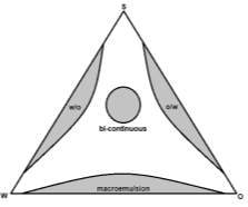 Microemulsions have become subject to a wide range of research including drug delivery systems, cleaning products and nanoparticle synthesis largely due to their intrinsic physiochemical properties of thermodynamic stability, small (variable) droplet size/large interfacial area, low polydispersity, low viscosity and optical isotropy.4 The formation of microemulsions is spontaneous under specific conditions controlled by the relative amounts of water, oil and surfactant – summarised in Figure 1.5
Figure 1: An example ternary phase diagram demonstrating the effect of relative amounts of water, oil and surfactant on microemulsion formation
Yes, completely! They’re a valid tool for getting sample papers to boost your own writing skills, and there’s nothing shady about that. Use them right—like a study guide or a model to learn from—and they’re a smart, ethical way to level up your grades without breaking any rules.
The surfactants used in microemulsion formation contain hydrophilic and hydrophobic ends, which will interact with the water and oil components respectively. In a w/o system, the hydrophilic heads of the surfactant will surround the water core and align the hydrophobic tails into the bulk oil. The interactions will stabilise the system and act to decrease surface tension (often to 10-3 dyne cm-1) allowing thermal motion to disperse the droplets – a spontaneous process. The formation of micelles can be described by the curvature free energy of the surfactant film in terms of its elasticity and shape. These properties are dependent on the nature of the surfactant (structure, intermolecular interactions) as well as the temperature and the presence of additives (alcohols, salts etc.).6 In relation to microemulsions use in nanoparticle synthesis, it is the control over droplet size which is key. The hydronamic radius, rH, of the droplet is linearly proportional to the ratio (w) of water: surfactant for a w/o system7
rH∝w=H2Osurfactant
Eq. 1
Prices start at $10 per page for undergrad work and go up to $21 for advanced levels, depending on urgency and any extras you toss in. Deadlines range from a lightning-fast 3 hours to a chill 14 days—plenty of wiggle room there! Plus, if you’re ordering big, you’ll snag 5-10% off, making it easier on your wallet while still getting top-notch quality.
Hence, control of these parameters produces aqueous droplets of a defined radius – optimal reactors for the synthesis of nanoparticles allowing manipulation of size, shape, surface area and homogeneity.
Production of nanoparticles from a mixture of reactants within a microemulsion requires the exchange of material between droplets. This is achieved through dynamic (Brownian) motion of the droplets within the microemulsion. Collisions between droplets result in the formation of fused dimers (or encounter pairs), reactant exchange and eventual dimer complex collapse. The rate at which these collisions occur is described by the exchange constant, kex. The inversion of film curvature at the interface (channel) between droplets impedes fusion, and is in turn dependent on the film elasticity – see Figure 2. 6
 Only once reactant material has been exchanged can a chemical reaction occur. Product particles begin to aggregate and form clusters. From this point, cluster growth occurs up to the limit set by the microemulsion droplet size and experimental conditions. Several growth mechanisms exist including ripening and autocatalysis.3, 8 Ostwald ripening (competitive growth) describes how nanoparticles will increase in size over time due to the increased stability of larger clusters vs. smaller clusters. A small cluster is more likely to dissolve into solution, which in turn becomes supersaturated leading to condensation onto a larger particle surface. Autocatalysis describes how a larger cluster may be able to catalyse the formation of nanoparticle products due to a larger surface area. These growth mechanisms are distinct from each other in that ripening is dependent on the inter-droplet exchange of product through the fused dimer channel whereas autocatalysis is dependent on reactant exchange/concentration. Hence, a rigid film can limit growth by ripening by reduction of channel size and limitation of reactant exchange.6, 9
Figure 2: A fused dimer system illustrating the exchange of reactants (green arrows) between droplets with inversion of film curvature (black arrows) promoting dimer collapse
Nope—your secret’s locked down tight. We encrypt all your data with top-tier security, and every paper’s crafted fresh just for you, run through originality checks to prove it’s one-of-a-kind. No one—professors, classmates, or anyone—will ever know you teamed up with us, guaranteed.
Surfactant adsorption onto the nanoparticle surface (capping) can also act to limit particle growth. Particularly common for catalytic particles (Pt, Pd, Rh etc.), this effect can be confirmed by uniform particle size independent of changes to synthetic conditions (reactant concentrations, excess). Recently microemulsions have been used to create nanoparticle clusters with a layered composition (e.g. Si-coated zinc ferrite) demonstrating unique magnetic properties.10 Our project focused on the use of microemulsions to create nanoparticles of ZnS, a classic Group II-VI semiconductor, in a range of sizes.
Semiconductors are defined as materials that have electrical conductance properties between fully conducting materials like gold or copper and insulators- wood or glass. Although these materials inherently do not possess and conductance properties with a band gap that is too large, this can be bridged through the manipulation of the material and its environment. By increasing the amount of impurity in a semiconductor material’s lattice structure we can alter its conductivity by a process known as “doping”. These doped semiconductors are known as “extrinsic”, and by varying the amounts of these impurities in these semiconductors conductivity can be varied factors of thousands or millions. The type of dopant material and its atomic properties define the properties of the semiconductor. Dopants that show these chosen properties are categorized as either being electron donors or acceptors; that being that p-type semiconductors contain acceptor impurities and n-type semiconductors being doped with donor type impurities, and these classifications indicate the type of charge carrier that is dominant in the substance.
Semiconductors have been used practically in electronics as the base for modern electrical equipment that contain electrical chips including radios, computers, and mobile phones as well as significantly before their introduction into the world of transistors as detectors in radios “cat’s whiskers”. In particular, Wide-bandgap II-VI semiconductors have found application in light-emitting devices for their photophysical and photochemical properties and their use at short wavelength regions close to visible light. This is in service to their bandgap energies and the ability to tune these properties using quantum size effects. The high ionicity of Wide-bandgap II-VI semiconductors opens them up for being good compounds for high electro-optical and electromechanical coupling.11
There are many methods that have been presented for the synthesis of high purity films and single crystals from both vapour and liquid phases of II-VI materials.
Not even a little—our writers are real-deal experts with degrees, crafting every paper by hand with care and know-how. No AI shortcuts here; it’s all human skill, backed by thorough research and double-checked for uniqueness. You’re getting authentic work that stands out for all the right reasons.
In Figure 3, we see a short summary of these methods of synthesis of large high-quality single crystals. Of these techniques; melt growth from the liquid phase was found to be the most time-efficient method of growing relatively large bulk crystals of II-VI semiconductors.11
Figure 3: Growth of bulk single crystals wide-bandgap II-VI compounds from the vapour, liquid and solid phases. From these methods include Chemical vapour transport (CVT) and Physical vapour transport (PVT) and liquid-phase methods including growth from the melt
Zinc sulfide (ZnS) is one of the first semiconductors discovered, very versatile in its properties and applications, including use in LED’s, lasers, sensors and IR windows.12
Our writers are Ph.D.-level pros who live for nailing the details—think deep research and razor-sharp arguments. We pair that with top plagiarism tools, free revisions to tweak anything you need, and fast turnarounds that don’t skimp on quality. Your research paper won’t just shine—it’ll set the bar.
 Synthesis of 0D ZnS nanoparticles; such as nanocrystals (quantum dots) has been successfully taking place since 1985 when Brus and co-workers developed a method using Na2S and Zn(ClO4)2 starting material at low temperatures.13 Although the synthesis was successful the particle sizes where very small and lacked tunability. Since then a more successful modern synthesis of II-VI materials was suggested by Bawendi and co-workers whose innovative method using hot trioctylphosphine oxide (TOPO) to form CdSe nanocrystals.14 This nonhydrolytic method was adapted by Hyeon and co-workers who were able to form ZnS nanocrystals from ZnCl and S in oleylamine in the presence of TOPO. This method by Hyeon and co-workers has become the most widely adopted method for synthesizing high-quality inorganic nanocrystals.15
Modern Semiconductors structures are described in terms of lattice structures, energies and quantum effects to get a true understanding of nanoparticle crystal lattices. Firstly, ZnS is generally referred as one of two different allotropes; these being Zincblende structure and wurtzite structure.
Notable differences arise from either in terms of their relative handedness of the fourth interatomic bond or by their dihedral conformations, or by the ABCABC pattern characteristic of the zinc blende coordinated atoms relative to the ABAB pattern observed for the wurtzite. In terms of dimensions according to reference for zinc blende; a = b = c = 5.41 Å, Z = 4 (space group F4-3 m) and that of WZ are a=b = 3.82 Å, c = 6.26 Å, Z = 2 (space group = P63mc).1 Although these differences are very slight the properties of both polymorphs can vary greatly.1 Zinc blend was found to have a band gap of 3.72eV and compared to wurtzite 3.77eV.
You’re in good hands with degree-holding pros—many rocking Master’s or higher—who’ve crushed our tough vetting tests in writing and their fields. They’re your partners in this, hitting tight deadlines and academic standards with ease, all while tailoring every essay to your exact needs. No matter the topic, they’ve got the chops to make it stellar.
Figure 4 (adapted from [1]): ZnS has two commonly available allotropes: one with a ZB structure and another with a WZ structure. The cubic form is the stable low-temperature phase, while the latter is the high-temperature polymorph which forms at around 1296 K.1 For the purpose of the comparison Fig. 2 shows three different views of these structures
In solid-state chemistry, the electronic band structure of a solid describes the range of energies or allowed bands that a single electron in a solid can access, as well as those it cannot have. Band theory derives these bands and band gaps for “allowed” or “forbidden” transitions and this governs both photosensitive and electronic properties of the solid. Band theory successfully explains physical properties such as conductivity of solids. Experimentally it has been shown that these different forms of ZnS are optically different. Authors state that mobility of electrons in these two forms is higher than that of holes since for both conduction-band minima are much more dispersive than the valence band maxima.16-20
These authors continue by stating electrons movement was more restricted than that of usual holes. P-electron in the highest valence band binds strongly to the sulfur restricting the band holes mobility and therefore restricts their impact on the conductivity. An experiment by Qadri and co using 2.7nm ZnS zinc blend nanoparticles and heated them at various temperatures showing that the temperature for the transition of the two allotropes, the bandgap energy and electronic structure considerably change when the size of the ZnS particles is of the order of nanometers.21
Experiments ran by Wang and co-workers calculated energy bandgaps of WZ-ZnS nanowires using DFT.22 ZnS nanowires were found to contain wider bandgaps than bulkier ZnS crystals and that the bandgap decreases inversely with diameter size. These results demonstrate the effect of quantum mechanics on the electronic structure and applications of Group II-VI semiconductors.
100%—we promise! Every paper’s written fresh from scratch—no AI, no copying—just solid research and proper citations from our expert writers. You can even request a plagiarism report to see it’s 95%+ unique, giving you total confidence it’s submission-ready and one-of-a-kind.
Quantum size effects occur when the dimensions of a solid have been drastically reduced. When the radii of particles are in the magnitude of nanometres, they become comparable to the de Broglie wavelength of the charge carriers (electrons and holes). At this scale, classical mechanics becomes inapplicable and quantum mechanics provides a better model of description. The charge carriers in the conduction band of these nanoparticles can be described by reduced dimensional models which create discrete energy levels. The energy gaps between these levels decrease as the dimensions reduce as well as increasing the surface area to volume ratio.
As a result of quantization, the energy gap is larger in quantum particles than it is in the bulk material which causes the interband transition to move to higher frequencies. If the band gap is increased too much the particle’s ability to conduct will reduce potentially to the point where no conduction is possible.
There are three types of reduced dimensionality systems: two-dimensional systems; one-dimensional systems and zero-dimensional systems.
Two-dimensional systems are very thin films, only a few nanometres thick and are generally deposited on top of a bulk material. The electrons are confined in the direction which is at a right angle to the film, however in the other two dimensions, which run parallel to the film the electrons are free to move as they would in the bulk material.23 An example of this is a quantum well.
Yep—APA, Turabian, IEEE, Chicago, MLA, whatever you throw at us! Our writers nail every detail of your chosen style, matching your guidelines down to the last comma and period. It’s all about making sure your paper fits academic expectations perfectly, no sweat.

The area that has a decreased energy is known as a well as it traps the holes and electrons which are drawn towards the area of lowest energy. They are formed when two semiconductors which have different bands gaps are fused together, creating a heterojunction. The difference in energy of the conduction and/or valence bands produces the well2. They provide a real-life example of the particle-in-a-box theory as the particle is confined along the z-axis due to the presence of barriers which have an infinitely high potential. The particle can along move along the z-axis by a fixed distance, Land is free to move inside the XY plane.
Figure 5: A quantum well
Figure 7: A quantum dot
Figure 6: A quantum wire
Absolutely—life happens, and we’re flexible! Chat with your writer anytime through our system to update details, tweak the focus, or add new requirements, and they’ll pivot fast to keep your paper on point. It’s all about making sure the final draft is exactly what you need, no stress involved.


One-dimensional systems are tubular objects with nanoscale diameters and micrometre lengths. It is also possible to have one-dimensional systems which contain a rectangular cross-section. These structures are confined in the transverse direction and electrons can only move in one direction.23 Quantum wires are an example of a one-dimensional system. These are made from quantum wells from lithography, followed by etching a single strip of material. They are used in electrical systems as transistors. These are typically in the range of 1 – 100 nm in radius.24
Zero-dimensional systems are made of a relatively small number of atoms (order of 103). The particles are unable to move as they are confined in all three directions. Examples of this type of system include fullerenes, clusters, nanocrystals and quantum dots.23 Dots are made from lithography and etching of quantum wells. They are also referred to as quantum boxes or nanocrystals. These are typically in the range of 1 – 10 nm in radius.24 The nanoparticles we plan to make are in this range. The radii of these dots can be calculated using the Brus equation:
ΔEr=Egap+h28r21me*+1mh*
It’s super easy—order online with a few clicks, then track progress with drafts as your writer works their magic. Once it’s done, download it from your account, give it a once-over, and release payment only when you’re thrilled with the result. It’s fast, affordable, and built with students like you in mind!
Where:
Egap is the energy of the bandgap.
h is Planck’s constant.
r is the radius of the dot.
We can crank out a killer paper in 24 hours—quality locked in, no shortcuts. Just set your deadline when you order, and our pros will hustle to deliver, even if you’re racing the clock. Perfect for those last-minute crunches without compromising on the good stuff.
me* is the mass of the electron which has been excited.
mh* is the mass of the excited hole.
The Brus equation demonstrates how the wavelength of the absorbed/emitted light changes with different radius lengths of the dots i.e. a decrease in particle size will increase the band-gap (reduced wavelength).25
Procedure:
Dried AOT (25.0 g, 56.2 mmol) and deoxygenated ZnCl2 (aq) solution (1.04 cm3, 1 M, 57.7 mmol H2O) were dissolved in heptane (1000 cm3) and mixed until optically clear. The solution was then deoxygenated with N2 gas. Finally, the solution was acidified with HCl (5 M).This procedure was repeated using deoxygenated Na2S (aq) solution (1.04 cm3, 1 M, 57.7 mmol H2O) and AOT (25.6 g, 57.5 mmol) (acidification released H2S (g).
For sure! Our writers with advanced degrees dive into any topic—think quantum physics or medieval lit—with deep research and clear, sharp writing. They’ll tailor it to your academic level, ensuring it’s thorough yet easy to follow, no matter how tricky the subject gets.
Deoxygenated stock ZnCl2 (aq) solution (0.23 cm3, 1 M) was made up to 100 cm3 by the addition of the already prepared ZnCl2 (aq) microemulsion solution. This procedure was then repeated using the deoxygenated stock Na2S (aq) solution (0.23 cm3, 1 M). This procedure was followed for the other w values using the volumes outlined below:
| Sample | r /nm | w (≈ r/0.18) | [H2O] / mol dm-3 | Additional Moles of H2O per 100 cm3 | Volume of Stock Reagent to be made up to 100 cm3 / cm3 |
| 1 | 0.6 | 3.3 | 0.1921 | 0.01345 | 0.23 |
| 2 | 1.2 | 6.7 | 0.3843 | 0.03266 | 0.57 |
| 3 | 1.8 | 10.0 | 0.5764 | 0.05188 | 0.90 |
| 4 | 2.4 | 13.3 | 0.7685 | 0.07109 | 1.23 |
Table 1: Summary of stock salt solution volumes required for each nanoparticle radius from the prepared w = 1 reverse-microemulsion solution.
The respective variable w cation and anion microemulsions were mixed. No colour change was observed contrary to expectation (ZnS = yellow). However, a white precipitate formed. This was agreed to likely be Zn(OH)2, formed due to the insufficient acidity of solutions and inherent basicity of Na2S (aq). Further acidification by conc. HCl did not result in the solvation of precipitate or colour change. No variation in this result was seen across sample range. Sample 4 (r = 2.4 nm) was repeated with freshly deoxygenated stock solutions and further HCl added to the stock solutions before addition of the microemulsion solution. Sample measured by UV-Vis spectroscopy. The sample set was placed in an ultrasonic bath to encourage droplet exchange and formation of ZnS. We observed no colour change indicating the presence of ZnS. All samples were analysed by UV-Vis spectroscopy; electronic absorption (200 – 700 nm) (Shimadzu UV-Visible Spectrometer).
A second generation of variable w reverse-microemulsion salt solutions was prepared using freshly deoxygenated stock solutions as described in Table 1 with acidification by HCl (5 M) prior to mixing. All samples were sonicated, sealed and left overnight. UV-Vis and fluorescence excitation/emission spectra were taken of all samples from this generation. A sample of each stabilised reverse-microemulsion was analysed against a blank of stock reverse-microemulsion. Each sample was measured as follows: electronic absorption (200 – 500 nm) (Shimadzu UV-Visible Spectrometer), fluorescence excitation (200 – 500 nm) and fluorescence emission (250 nm) (Perkin Elmer Fluorescence Spectrometer) – identifying maxima and trends relating to particle size. Each particle size was tested twice using a fresh sample.
AOT was purified by solvation in petroleum ether, filtration and evaporating to dryness. A third set of variable w reverse-microemulsion salt solutions was prepared using the procedure outlined above. However, only half the volume of reverse-microemulsion (w = 1) salt solutions was prepared. Dried AOT (12.8 g, 28.8 mmol), (12.8 g, 28.9 mmol) was added to the Na2S and ZnCl2 solutions respectively. The variable w cation and anion microemulsions were then mixed. Sample 3 of this generation was sonicated. Electronic absorption spectra were then taken for a range of samples before inspection led us to conclude the absence of ZnCl2 from the ZnCl2 (aq) (w = 1). AgNO3 (aq) test of a sample from the ZnCl2 (aq) (w = 1) solution was inconclusive. As such small volumes of ZnCl (aq) were used; precipitation may not have been visually obvious. Our group agreed that this was the likely cause of the unexpected spectra and proceeded to correct the mistake by addition of the required quantities of ZnCl2 (aq) to the respective samples of generation 3. UV-Vis and fluorescence spectra were carried out on selected samples but it was clear that the addition of ZnCl2 (aq) had not corrected the issue and generation 3 was disregarded.
We stick to your rubric like glue—nailing the structure, depth, and tone your professor wants—then polish it with edits for that extra shine. Our writers know what profs look for, and we double-check every detail to make sure it’s submission-ready and grade-worthy.
 Results:
Figure 8: Graph showing the electronic absorption spectrum for Sample 1, Generation 1, Run 1
Send us your draft and tell us your goals—we’ll refine it, tightening arguments and boosting clarity while keeping your unique voice intact. Our editors work fast, delivering pro-level results that make your paper pop, whether it’s a light touch-up or a deeper rework.
Yes—we’ve got your back! We’ll brainstorm fresh, workable ideas tailored to your assignment, picking ones that spark interest and fit the scope. You choose the winner, and we’ll turn it into a standout paper that’s all yours.
Yep—need changes fast? We’ll jump on your paper and polish it up in hours, fixing whatever needs tweaking so it’s ready to submit with zero stress. Just let us know what’s off, and we’ll make it right, pronto.
Figure 9: Graph showing the electronic absorption spectrum for Sample 2, Generation 1, Run 1
Sure thing! We’ll whip up a clear outline to map out your paper’s flow—key points, structure, all of it—so you can sign off before we dive in. It’s a handy way to keep everything aligned with your vision from the start.
Absolutely—we’ll weave in sharp analysis or eye-catching visuals like stats and charts to level up your paper. Whether it’s crunching numbers or designing a graph, our writers make it professional and impactful, tailored to your topic.
Figure 10: Graph showing the electronic absorption spectrum for Sample 3, Generation 1, Run 1
Yes—we’ve got it down! Our writers switch seamlessly between UK, US, Australian, or any other standards, matching your school’s exact expectations. Your paper will feel native to your system, polished and ready for wherever you’re studying.
Progressive delivery is a cool option where we send your paper in chunks—perfect for big projects like theses or dissertations. You can even pay for it in installments. It’s just 10% extra on your order price, but the perks are worth it. You’ll stay in closer touch with your writer and can give feedback on each part before they move to the next. That way, you’re in the driver’s seat, making sure everything lines up with what you need. It saves time too—your writer can tweak things based on your notes without having to redo huge sections later.
Figure 11: Graph showing the electronic absorption spectrum for Sample 4, Generation 1, pre-sonication
Absolutely! If your teacher’s got feedback, you can request a free revision within 7 days of approving your paper—just hit the revision request button on your personal order page. Want a different writer to take a crack at it? You can ask for that too, though we might need an extra 12 hours to line someone up. After that 7-day window, free revisions wrap up, but you can still go for a paid minor or major revision (details are on your order page). What if I’m not satisfied with my order? If your paper needs some tweaks, you’ve got that free 7-day revision window after approval—just use the “Revision” button on your page. Once those 7 days are up, paid revision options kick in, and the cost depends on how much needs fixing. Chat with our support team to figure out the best way forward. If you feel the writer missed the mark on your instructions and the quality’s off, let us know—we’ll dig in and sort it out. If revisions don’t cut it, you can ask for a refund. Our dispute team will look into it and figure out what we can offer. Check out our money-back guarantee page for the full scoop.
Figure 12: Graph showing the electronic absorption spectrum for Sample 4, Generation 1, post-sonication
Figure 13: Graph showing the electronic absorption spectrum for Sample 1, Generation 2, Run 1
Figure 14: Graph showing the electronic absorption spectrum for Sample 2, Generation 2, Run 1
Figure 15: Graph showing the electronic absorption spectrum for Sample 3, Generation 2, Run 1
Figure 16: Graph showing the electronic absorption spectrum for Sample 4, Generation 2, Run 1
Figure 17: Graph showing the electronic absorption spectrum for Sample 3, Generation 3, Run 1
Figure 18: Graph showing the electronic absorption spectrum for Sample 2, Generation 3, Run 4
Figure 19: Fluorescence spectra for Generation 2 (no change across generation)

Analysis:
Figure 20: Fluorescence Emission Spectrum for Sample 3, Generation 1, Run 1
Figure 21: Fluorescence Emission Spectrum for Sample 3, Generation 3, Run 1
The electronic absorption spectra for was analysed using the cut-on method outlined below:

Figure 22: An illustration showing how to find the cut-on point for sample 1, generation 2, run 1.
| Wavelength (nm) | Absorbance |
| 298 | 0.2386 |
| 300 | 0.2303 |
| 303 | 0.2180 |
| 305 | 0.2094 |
| 312 | 0.1809 |
Table 2: The data points used to deduce the equation of the tangent for sample 1, generation 2, run 1.
Figure 22: A graph showing the tangent line used to deduce the cut-on point for sample 1, generation 2, run 1.
Equation of tangent:
y=-0.0042x+1.4784
Equation of baseline:
y=0.0374
Point where these two lines meet:
0.0374=-0.0042x+1.4784
-1.441=-0.0042x
x=-1.441-0.0042
x=343
The cut-on point for sample 1, generation 2, run 1 is 343 nm.
| Generation | Sample | Run | Equation of tangent | Value of y | Cut-on point (nm) |
| 1 | 1 | 1 | – | – | – |
| 1 | 1 | 2 | – | – | – |
| 1 | 2 | 1 | y=-0.0020x+0.7117 | 0.0448 | 333 |
| 1 | 2 | 2 | y=-0.0060x+1.4784 | 0.1722 | 411 |
| 1 | 3 | 1 | y=-0.0026x+0.9268 | 0.0834 | 324 |
| 1 | 3 | 2 | y=-0.0021x+0.6512 | -0.0632 | 340 |
| 1 | 4 | 1 | y=-0.0318x+11.8520 | 0.3987 | 360 |
| 1 | 4 | 2 | y=-0.0236x+8.6762 | 0.1913 | 360 |
| 2 | 1 | 1 | y=-0.0042x+1.4784 | 0.0374 | 343 |
| 2 | 1 | 2 | y=-0.0065x+1.4784 | 1.0833 | 357 |
| 2 | 2 | 1 | y=-0.0039x+1.2459 | -0.0515 | 333 |
| 2 | 2 | 2 | y=-0.0031x+1.1280 | 0.0115 | 360 |
| 2 | 3 | 1 | y=-0.0122x+4.8046 | 0.2781 | 371 |
| 2 | 3 | 2 | y=-0.0111x+4.0520 | 0.1758 | 349 |
| 2 | 4 | 1 | y=-0.0107x+3.9564 | 0.1961 | 351 |
| 2 | 4 | 2 | y=-0.0112x+4.3451 | 0.3168 | 360 |
| 2 | 4 | 3 | y=-0.0107x+3.8395 | 0.1158 | 348 |
| 2 | 4 | 4 | y=-0.0105x+3.5772 | 0.0153 | 339 |
| 3 | 3 | 1 | y=-0.0430x+14.9600 | 0.9824 | 325 |
| 3 | 3 | 2 | y=-0.0057x+3.8104 | 1.6649 | 376 |
Table 3: Cut-on point for the three generations of semi-conductor particles.
| Radius of Particle (nm) | Average Cut-on Point (nm) |
| 0.6 | 350.0 |
| 1.2 | 346.5 |
| 1.8 | 360.0 |
| 2.4 | 349.5 |
Table 4: Average cut-on points for generation 2.
Figure 23: Graph of the average cut-on point for generation 2 against the radius of the particles formed
.
Discussion:
Our group attempted the synthesis of ZnS nanoparticles using literature methods that had been successful in producing nanoparticle of discrete radii with low polydispersity.7, 26 However, we did not achieve the formation of ZnS nanoparticles by reverse-microemulsion synthesis as demonstrated by Figure 17. The average cut-on values and therefore band-gaps for the range of particle sizes our group attempted to produce show no size/band-gap correlation (quantum size effect) as well as no significant change from the bulk ZnS electronic structure. The band-gap variation covers only the small range of 346.5 – 360 nm which corresponds to 3.44 – 3.58 eV (E=hc/ν).
Bulk ZnS has a band gap of approx. 3.6 – 3.7 eV (dependent on crystal structure)1 whereas nanoparticles of a 20 – 30 nm radius show an increased gap of 4.03eV. 27This broadening of the band-gap can be described by the Brus equation
∆Er=Egap+h28r2(1me*+1mh*)
By comparison of these radii/bulk band-gaps and the Brus equation, it can safely be assumed that the band-gap of nanoparticles in the range of 0.5 – 2.5 nm would be greater than 4.03 eV (E inversely proportional to r2).
Failure to form ZnS nanoparticles could be attributed to several issues with the synthetic procedure. The reaction of Zn2+(aq) with S2-(aq) requires both components to be available in sufficient concentrations within the aq. micelles. Na2S (aq) is a weak base and can abstract protons from water to form HS– leading to H2S, which although soluble in water can be released into the atmosphere (evidenced by a rotten egg smell). This would lead to a decreased concentration of S-2(aq) available for reaction. On the other hand, Zn2+(aq) in basic solution forms Zn(OH)2 which is insoluble in water and therefore precipitates out and removes Zn2+(aq) from solution. It should be noted that although we describe S-2, it has been shown to not exist in even strongly basic solutions (through Raman spectra analysis) instead of existing as HS–.28 However, for the purpose of this report and sulphide’s role in the formation of ZnS, we will describe it as S-2.
Our group acidified (HCl) the stock solutions before mixing in order to limit this precipitation but this may have led to the loss of S-2 from solution as previously described. A fine pH balance is therefore required to ensure minimal loss of either Zn2+ or S-2 from solution, which our group may not have achieved leading to the poor formation of ZnS.
Insufficient deoxygenation of the stock solutions may have also played a part in the lack of ZnS formed. S-2 in the presence of dissolved O2 can oxidise to S or SO42- leading to a decreased concentration available for reaction with Zn2+.
These theories may explain only a small amount of ZnS being formed however they do not justify the formation of bulk ZnS over nanoparticles. For this to have occurred there must have been a flaw in the formation of the microemulsion e.g. no micelle formation or the radius of micelles that formed were too large and did not limit the growth of nanoparticles as anticipated. The simplest explanation for this relates to the amount of water present and therefore w values of the solution produced. Too much water would produce a w value greater than expected
rH∝w=H2Osurfactant
A larger w would, therefore, result in the larger micelles and the formation of (nano)particles greater in size than originally predicted. As the quantities of AOT (surfactant) were controlled to a greater degree (large mass ~ 25 g, any slight change (e.g. ± 0.1 g would not significantly affect the ratio). Above a certain particle radius, the quantum size effect described by the Brus equation would no longer apply and the band-gap would be more alike to that of the bulk material than a nanoparticle. This theory would help to explain the lack of distinction between our synthesised nanoparticles and the literature band-gap value of ZnS. The small (non-linear) variation between band-gaps for our results could be assumed to be due to a degree of microemulsion size control beyond nanoparticle radii i.e. 1.8 nm result (smallest apparent band-gap) having a larger actual w value than the 2.4 nm result (larger apparent band-gap). The variation in w values could be attributed to the acidification with HCl step in the synthetic procedure and the amount of water present in the aqueous acid.
The spectral data we gathered did not match our expectations based on the literature review we undertook. Only the UV absorption spectra for the second generation provided interpretable data and allowed us to come to the conclusion that the synthesis of ZnS nanoparticles did not proceed. The absorption data for the first and third generation was not consistent with each other and the literature. The fluorescence spectra for the third generation was the same across all sample sizes. This could be attributed to the formation of bulk ZnS rather than nanoparticles as previously discussed or may have to due to our own error in the set-up of the fluorescence spectrometer parameters/error in the saving of files.
Conclusion
1. C.-Y. Yeh, Z. Lu, S. Froyen and A. Zunger, Physical Review B, 1992, 46, 10086.
2. J. H. Schulman, W. Stoeckenius and L. M. Prince, The Journal of Physical Chemistry, 1959, 63, 1677-1680.
3. M. A. Malik, M. Y. Wani and M. A. Hashim, Arabian Journal of Chemistry, 2012, 5, 397-417.
4. J. Klier, C. J. Tucker, T. H. Kalantar and D. P. Green, Advanced Materials, 2000, 12, 1751-1757.
5. H. S. GK Sahu, A Gupta, CD Kaur, International Journal of Pharmaceutical Sciences and Developmental Research, 2015, 15, 008-015.
6. M. A. López-Quintela, Current Opinion in Colloid & Interface Science, 2003, 8, 137-144.
7. C. Petit and M. P. Pileni, The Journal of Physical Chemistry, 1988, 92, 2282-2286.
8. C. Tojo, M. d. Dios and F. Barroso, Materials, 2011, 4, 55.
9. M. L. Curri, A. Agostiano, L. Manna, M. D. Monica, M. Catalano, L. Chiavarone, V. Spagnolo and M. Lugarà, The Journal of Physical Chemistry B, 2000, 104, 8391-8397.
10. F. Grasset, N. Labhsetwar, D. Li, D. C. Park, N. Saito, H. Haneda, O. Cador, T. Roisnel, S. Mornet, E. Duguet, J. Portier and J. Etourneau, Langmuir, 2002, 18, 8209-8216.
11. S. Kasap and P. Capper, Springer Handbook of Electronic and Photonic Materials, Springer, 2006.
12. W. Davidson, Phys Rev, 1948, 74, 116-117.
13. R. Rossetti, R. Hull, J. Gibson and L. E. Brus, The Journal of chemical physics, 1985, 82, 552-559.
14. C. Murray, D. J. Norris and M. G. Bawendi, Journal of the American Chemical Society, 1993, 115, 8706-8715.
15. J. Joo, H. B. Na, T. Yu, J. H. Yu, Y. W. Kim, F. Wu, J. Z. Zhang and T. Hyeon, Journal of the American Chemical Society, 2003, 125, 11100-11105.
16. S. Z. Karazhanov, P. Ravindran, A. Kjekshus, H. Fjellvåg and B. Svensson, Physical Review B, 2007, 75, 155104.
17. C.-Y. Yeh, S.-H. Wei and A. Zunger, Physical Review B, 1994, 50, 2715.
18. S. Adachi, Journal, 1999.
19. S. Z. Karazhanov, A. Ulyashin, P. Ravindran and P. Vajeeston, EPL (Europhysics Letters), 2008, 82, 17006.
20. S. Z. Karazhanov, P. Ravindran, A. Kjekhus, H. Fjellvåg, U. Grossner and B. Svensson, Journal of crystal growth, 2006, 287, 162-168.
21. S. Qadri, E. Skelton, D. Hsu, A. Dinsmore, J. Yang, H. Gray and B. Ratna, Physical Review B, 1999, 60, 9191.
22. J. Li and L.-W. Wang, Physical Review B, 2005, 72, 125325.
23. K. Pedersen, Quantum Size Effects in Nanostructures [lecture notes], Aalborg University, http://homes.nano.aau.dk/kp/Quantum%20size%20effects%20in%20nanostructures.pdf (accessed 20 February 2018),
24. B. G. J. R. J. B. Balaguru, Quantum Wells, Quantum Wires, Quantum Dots, Quantum Limit of Conductance, Quantum Capacitance & Quantum Hall Effect, SASTRA University, http://nptel.ac.in/courses/115106076/Module%207/Module%207.pdf
25. L. Brus, The Journal of Physical Chemistry, 1986, 90, 2555-2560.
26. C. Petit, P. Lixon and M. Pileni, Journal of Physical Chemistry, 1990, 94, 1598-1603.
27. A. Chandran, N. Francis, T. Jose and K. George, Acad Rev, 2010, 17, 17-21.
28. P. M. May, D. Batka, G. Hefter, E. Konigsberger and D. Rowland, Chemical Communications, 2018, 54, 1980-1983.
Tags: Assessment Brief Assignment Help, Australia dissertation writers, Help write my thesis paper in UK, I need help with my HomeworkYou Want The Best Grades and That’s What We Deliver
Our top essay writers are handpicked for their degree qualification, talent and freelance know-how. Each one brings deep expertise in their chosen subjects and a solid track record in academic writing.
We offer the lowest possible pricing for each research paper while still providing the best writers;no compromise on quality. Our costs are fair and reasonable to college students compared to other custom writing services.
You’ll never get a paper from us with plagiarism or that robotic AI feel. We carefully research, write, cite and check every final draft before sending it your way.