
Top Essay Writers
Our top essay writers are handpicked for their degree qualification, talent and freelance know-how. Each one brings deep expertise in their chosen subjects and a solid track record in academic writing.
Simply fill out the order form with your paper’s instructions in a few easy steps. This quick process ensures you’ll be matched with an expert writer who
Can meet your papers' specific grading rubric needs. Find the best write my essay assistance for your assignments- Affordable, plagiarism-free, and on time!
Posted: September 15th, 2022
The report is based on the Digital Implementation of Phase locked loop on FPGA, the report covers the steps taken for implementing the proposed Phase Locked loop architecture on the FPGA. The building blocks used for the architecture are explained in detail as well as the software and technologies used for the project. An extensive literature research has also been done on past designs of the PLL and its contribution to this project is explained. Finally, the results gotten from the software and hardware will also be analysed.
We hear “Can you write in APA or MLA?” all the time—and the answer’s a big yes, plus way more! Our writers are wizards with every style—APA, MLA, Harvard, Chicago, Turabian, you name it—delivering flawless formatting tailored to your assignment. Whether it’s a tricky in-text citation or a perfectly styled reference list, they’ve got the skills to make your paper academically spot-on.
Yes, completely! They’re a valid tool for getting sample papers to boost your own writing skills, and there’s nothing shady about that. Use them right—like a study guide or a model to learn from—and they’re a smart, ethical way to level up your grades without breaking any rules.
Prices start at $10 per page for undergrad work and go up to $21 for advanced levels, depending on urgency and any extras you toss in. Deadlines range from a lightning-fast 3 hours to a chill 14 days—plenty of wiggle room there! Plus, if you’re ordering big, you’ll snag 5-10% off, making it easier on your wallet while still getting top-notch quality.
2.1. BUILDING BLOCKS OF PHASE LOCKED LOOP
Nope—your secret’s locked down tight. We encrypt all your data with top-tier security, and every paper’s crafted fresh just for you, run through originality checks to prove it’s one-of-a-kind. No one—professors, classmates, or anyone—will ever know you teamed up with us, guaranteed.
2.1.3 VOLTAGE CONTROLLED OSCILLATOR
2.2. TYPES OF PHASE LOCKED LOOP
2.3. TECHNOLOGY AND DESIGN TOOLS
Not even a little—our writers are real-deal experts with degrees, crafting every paper by hand with care and know-how. No AI shortcuts here; it’s all human skill, backed by thorough research and double-checked for uniqueness. You’re getting authentic work that stands out for all the right reasons.
2.3.2. XILINX SYSTEM GENERATOR FOR DSP
2.4. FPGA BASED PLL BASED ON RANDOM SAMPLING
Our writers are Ph.D.-level pros who live for nailing the details—think deep research and razor-sharp arguments. We pair that with top plagiarism tools, free revisions to tweak anything you need, and fast turnarounds that don’t skimp on quality. Your research paper won’t just shine—it’ll set the bar.
2.4.2. ARCHITECTURE OF PROPOSED DESIGN
2.4.3. IMPLEMENTATION OF EACH BLOCK
2.5. FPGA BASED PLL WITH WIRELESS TRANSCEIVER ARCHITECTURE TESTING
You’re in good hands with degree-holding pros—many rocking Master’s or higher—who’ve crushed our tough vetting tests in writing and their fields. They’re your partners in this, hitting tight deadlines and academic standards with ease, all while tailoring every essay to your exact needs. No matter the topic, they’ve got the chops to make it stellar.
100%—we promise! Every paper’s written fresh from scratch—no AI, no copying—just solid research and proper citations from our expert writers. You can even request a plagiarism report to see it’s 95%+ unique, giving you total confidence it’s submission-ready and one-of-a-kind.
2.6. COMPARISON OF CASE STUDIES
2.7. CONTRIBUTIONS TO CURRENT WORK
2.8. NUMERICALLY CONTROLLED OSCILLATOR
Yep—APA, Turabian, IEEE, Chicago, MLA, whatever you throw at us! Our writers nail every detail of your chosen style, matching your guidelines down to the last comma and period. It’s all about making sure your paper fits academic expectations perfectly, no sweat.
Absolutely—life happens, and we’re flexible! Chat with your writer anytime through our system to update details, tweak the focus, or add new requirements, and they’ll pivot fast to keep your paper on point. It’s all about making sure the final draft is exactly what you need, no stress involved.
3.2. PROPOSED SYSTEM ARCHITECTURE
It’s super easy—order online with a few clicks, then track progress with drafts as your writer works their magic. Once it’s done, download it from your account, give it a once-over, and release payment only when you’re thrilled with the result. It’s fast, affordable, and built with students like you in mind!
3.2.3. NUMERICALLY CONTROLLED OSCILLATOR
We can crank out a killer paper in 24 hours—quality locked in, no shortcuts. Just set your deadline when you order, and our pros will hustle to deliver, even if you’re racing the clock. Perfect for those last-minute crunches without compromising on the good stuff.
3.3.4. NUMERICALLY CONTROLLED OSCILLATOR TEST
For sure! Our writers with advanced degrees dive into any topic—think quantum physics or medieval lit—with deep research and clear, sharp writing. They’ll tailor it to your academic level, ensuring it’s thorough yet easy to follow, no matter how tricky the subject gets.
APPENDIX A: PROPOSED PLL DESIGN
We stick to your rubric like glue—nailing the structure, depth, and tone your professor wants—then polish it with edits for that extra shine. Our writers know what profs look for, and we double-check every detail to make sure it’s submission-ready and grade-worthy.
APPENDIX B: DIGITAL FILTER TEST DESIGN
APPENDIX C: PHASE DETECTOR TEST DESIGN
APPENDIX D: NUMERICALLY CONTROLLED OSCILLLATOR TIME DOMAIN TEST
Figure 1: Basic Structure of Phase locked Loop
Send us your draft and tell us your goals—we’ll refine it, tightening arguments and boosting clarity while keeping your unique voice intact. Our editors work fast, delivering pro-level results that make your paper pop, whether it’s a light touch-up or a deeper rework.
Figure 3: Design Flow for System generator for DSP
Figure 4: Logical Diagram of 16-Bit pseudo-random number generator
Figure 6: Square Wave input frequency test. [14]
Yes—we’ve got your back! We’ll brainstorm fresh, workable ideas tailored to your assignment, picking ones that spark interest and fit the scope. You choose the winner, and we’ll turn it into a standout paper that’s all yours.
Figure 7: Sinusoidal input frequency test [14]
Figure 8: Simulink model of the ADPLL [12]
Figure 9: Proposed design of phase detector and loop filter
Figure 10: Simulated results of the ADPLL design[12].
Figure 11: Simulated Result for the NCO outputs I_feedback and Q_feedback [12].
Figure 12: The ADPLL set up [12].
Figure 13: I-Q constellation transmitted with the input signal of 2.4 GHz [12]
Yep—need changes fast? We’ll jump on your paper and polish it up in hours, fixing whatever needs tweaking so it’s ready to submit with zero stress. Just let us know what’s off, and we’ll make it right, pronto.
Figure 14: I-Q constellation recovered by the proposed ADPLL with the input signal of 2.4 GHz [12]
Figure 15: CORDIC Vector Rotation Diagram
Figure 16: 2nd order IIR Filter for generating sine wave
Figure 17: Block Diagram for LUT Based NCO[19].
Figure 18: Flow Chart describing whole project
Figure 19: Proposed Architecture of PLL
Sure thing! We’ll whip up a clear outline to map out your paper’s flow—key points, structure, all of it—so you can sign off before we dive in. It’s a handy way to keep everything aligned with your vision from the start.
Figure 20: Response Curve for XOR Phase Detector [16].
Figure 21: Subsystem of Proposed NCO
Figure 22: Digital Filter test schematic
Figure 23: Output of Digital Filter with a 1Hz Input Signal
Figure 24: Phase Detector testing schematic
Figure 25: input signals with equivalent phases;
Figure 26: Difference in phase between the two input signals
Figure 27: Output of the PLL (Input Signal and Generated output signal)
Absolutely—we’ll weave in sharp analysis or eye-catching visuals like stats and charts to level up your paper. Whether it’s crunching numbers or designing a graph, our writers make it professional and impactful, tailored to your topic.
Figure 28: Spectrum analyser view of the NCO output
Table 1: Parameter Values of Digital Filter
Table 2: Parameter values of two input signals
We tackle each chunk with precision, keeping quality consistent and deadlines on track from start to finish. Whether it’s a dissertation or a multi-part essay, we stay in sync with you, delivering top-notch work every step of the way.
Table 3: Table Comparison between Input Signal and NCO output
| ABBREVIATION | MEANING |
| PLL | Phase Locked Loop |
| ADPLL | All-Digital Phase Locked Loop |
| VCO | Voltage Controlled Oscillator |
| MATLAB | Matrix Laboratory |
| FPGA | Field Programmable Gate Array |
| DSP | Digital Signal Processing |
| VHDL | VHSIC Hardware Description Language |
| RTL | Register Transfer Level |
| CDMA | Code Division Multiple Access |
| PI | Proportional Integrator |
| QPSK | Quadrature Phase Shift Keying |
| QAM | Quadrature Amplitude Modulation |
| BET | Bit Error Rate |
| NCO | Numerically Controlled Oscillator |
| ARS | Addictive Random Sampling |
| ADC | Analog to Digital Converter |
| DAC | Digital to Analog Converter |
| CORDIC | COordinate Rotation DIgital Computer |
| IIR | Infinite Impulse Response |
| DDS | Digital Design Synthesizer |
| FIR | Finite Impulse Response |
| LUT | Look-Up Table |
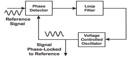
Phase Locked loop is a control system which has an input signal that is synchronized in frequency and phase with a generated output signal gotten from a control oscillator. This means the PLL will be in a locked condition when the input signal and the output signal have zero or very small difference between there frequency and phase. Phase locked loop usually comprises of voltage controlled oscillator, phase detector or comparator and a low pass filter. The oscillator produces a periodic signal. The phase detector compares the phase of the input periodic signal with the phase of the produced/generated periodic signal and modifies the oscillator to keep the phases synchronized. The PLL is classified as a feedback loop system due to the fact that it takes an output signal towards the input signal for a comparison in a loop.
Yes—we’ve got it down! Our writers switch seamlessly between UK, US, Australian, or any other standards, matching your school’s exact expectations. Your paper will feel native to your system, polished and ready for wherever you’re studying.
PLL’s are used in a variety of applications such as AM and FM Modulation, Frequency multiplication, Clock distribution and recovery and also jitter and noise reduction. They are also used in demodulating a signal, recovering a signal from a noisy communication channel and generate a stable frequency at multiples of an input frequency or distribute precisely timed clock pulses in digital logic circuits , for example a microprocessor [1].
The sole aim of this project is to design a digitally based phased locked loop which can be implemented on an FPGA, the preferable type of PLL to use in this case is the All-Digital PLL which was discussed earlier. The reason being is due to the fact that all building blocks are digitally based. The aim of this report is to explain in details how the All-Digital PLL was modelled on Xilinx System Generator for DSP software and how it was eventually synthesized onto the FPGA. The project workload has been subdivided into various objectives which includes;
An extensive literature research has been performed on the phase locked loop and it has been seen that its building blocks have various ways it could be implemented and also different digital and analog counterparts. This section will take an in-depth analysis of each of these blocks which will include the theory behind each of them, case studies, equations and diagrams etc. This section will also take an analysis of some related case studies and its contribution to the current project. An explanation on the devices required for the project have also been covered.
The typical phase locked loop has three main building blocks in the design as stated in section 1. These blocks are mainly;
Progressive delivery is a cool option where we send your paper in chunks—perfect for big projects like theses or dissertations. You can even pay for it in installments. It’s just 10% extra on your order price, but the perks are worth it. You’ll stay in closer touch with your writer and can give feedback on each part before they move to the next. That way, you’re in the driver’s seat, making sure everything lines up with what you need. It saves time too—your writer can tweak things based on your notes without having to redo huge sections later.
This is the part of the PLL that is responsible for the comparing of the input signal and the generated output signal to determine whether or not both signals have similar phase and frequencies. This part of the PLL has the most significance due to the fact that is solely responsible for determining the phase difference in the loop and it also detects the resulting error in the PLL if there is any. In order for a better understanding of this block, assume there is a frequency of any random value, if the Fin≠ Fgen, the phase-error signal, after being filtered and amplified, causes the generated frequency to deviate in the direction of the of Fin[2]. If the conditions are right, the generated frequency will quickly lock to Fin, maintaining a fixed phase relationship with the input signal [2].
This part of the PLL will remove unnecessary high frequencies which could pass out of the phase detector and go through the VCO. From Figure 1-1, it is seen that there is a reference signal in the block diagram which contains sum and difference frequency components which are often times called high and low frequency components respectively. The PLL will only require the high frequency components and it is the duty of the low pass filter to cut-off the low frequency components from the phase detector so the signal can be passed to the VCO. Thereafter, the input signal and reference signal will be locked in phase and frequency
This block will feed the generated output signal to the phase detector to determine whether it is in phase with the input signal. The frequency of the output signal of the VCO is controlled by the input voltage driven into it. This input voltage will define the oscillation frequency. Consequently, modulated signals connected to the input signals may cause frequency modulation (FM) or phase modulation (PM). VCO can have a sine wave, square wave, ramp wave as its output but it’s solely dependent on the input signal driven into the phase locked loop. Analog based phase locked loop normally uses the VCO while the digitally based phase locked loop contains the VCO’s digital counterpart called a Numerically Controlled Oscillator (NCO) or in a semi-digital phase locked loop called a Digitally Controlled Oscillator (DCO).
Absolutely! If your teacher’s got feedback, you can request a free revision within 7 days of approving your paper—just hit the revision request button on your personal order page. Want a different writer to take a crack at it? You can ask for that too, though we might need an extra 12 hours to line someone up. After that 7-day window, free revisions wrap up, but you can still go for a paid minor or major revision (details are on your order page). What if I’m not satisfied with my order? If your paper needs some tweaks, you’ve got that free 7-day revision window after approval—just use the “Revision” button on your page. Once those 7 days are up, paid revision options kick in, and the cost depends on how much needs fixing. Chat with our support team to figure out the best way forward. If you feel the writer missed the mark on your instructions and the quality’s off, let us know—we’ll dig in and sort it out. If revisions don’t cut it, you can ask for a refund. Our dispute team will look into it and figure out what we can offer. Check out our money-back guarantee page for the full scoop.
There are different variations of the phase locked loop which can have either analogically or digitally based building blocks, these include;
The term FPGA stands for Field Programmable Gate Array. An FPGA is an integrated circuit system which can be programmed or configured to the required functionality of the user. They are widely used in many industries for different purposes such as digital signal processing, media imaging, speech recognition, consumer electronics, military and aerospace. Due to these various applications this makes the FPGA more economical and marketable. Different companies such Xilinx Inc., Lattice Semiconductor and Altera Corporation are some of the top leading manufactures and accounted for more than 80% of the global FPGA market share in 2014[3].
The internal structure of an FPGA contains a programmable logic blocks such as AND & XOR, I/O cells which connects the logic cells to external signals and a programmable routing network interconnecting the cells. The FPGA are programmed using Hardware Description language such as Verilog and VHDL.
System Generator is a DSP design tool from Xilinx that uses MathWorks model based Simulink design environment for FPGA design [7]. Past experience with Xilinx FPGA or RTL design approaches are not requires when utilizing system generator. Designers can develop and simulate a model using MATLAB, Simulink and Xilinx library of bit or cycle-true models. Xilinx pre-advanced algorithm are then mapped from the synthesizable hardware description language (HDL) which are made automatically from the tool. The HDL design will then be integrated for implementation on Xilinx FPGA and any other programmable SoCs. Subsequently, designers can characterize conceptual representation of a system-level design and effortlessly change this single source code into a gate level portrayal. Also, it gives a programmed generation of a HDL test bench, which can enable design to be verified after implementation. The figure below is a flow chart that summarizes the flow of a Simulink design to the implementation to the FPGA.
Figure 3: Design Flow for System generator for DSP
The level of abstraction given by System Generator for DSP has significantly clarified algorithm development. Besides the system-level modelling library, System generator incorporates a code generator that can automatically produces a synthesizable VHDL netlist from a Simulink model. This netlist contains IP (Intellectual property) that have been designed specifically for high level performance and density in Xilinx FPGA. System generator creates project and constraints file to assist implementation using Xilinx foundation as the major synthesis tool [11].
It is well known that digitally based PLL are only compatible with low frequency based applications and cannot be processed with high frequency based applications. This is due to the fact that at high frequencies, there are a lot of mathematical calculations which restricts the functioning in a DSP system. Also the analog to digital converter (ADC) restricts the speed of DSP systems [4]. The proposed PLL based on random sampling is brought about by the idea of been able to use random sampling to process high frequency analog signals at frequencies lower than the Nyquist frequency without having an aliasing effect. Aliasing effect on a signal occurs when a signal is been sampled at a frequency similar or even smaller than the signal being measured.
The PLL in this section follows the typical concept of a basic PLL were the components are the input signal, phase detector (PD), the loop filter, VCO and output signal. A sine wave is used as the input signal of the design. The phase detector generates a signal formed by the phase error which is added by other non-desired parts, for example, the high frequency harmonics originating from the non-linear components (i.e. multiplication) and arbitrary noise. The filter will sift out these redundant components and will just keep the phase error signal. The filter also functions as a controller in the closed loop system, which attempts to decrease the phase error signal to zero. The Proportional Integral (PI) is a good example of a filter that meets these necessities. The gain constants within the PI design can determine how far the locking time is and the range between each period of the output signal.
The sampling type methodology used in this design is called Addictive random sampling (ARS). This is a type of sampling methodology intended to provide alias-free processing of random signals [13]. The input signal driven into the phase detector of the proposed design is sampled at random moments which are characterised by the equation shown below;
| ti+1 |
You Want The Best Grades and That’s What We Deliver
Our top essay writers are handpicked for their degree qualification, talent and freelance know-how. Each one brings deep expertise in their chosen subjects and a solid track record in academic writing.
We offer the lowest possible pricing for each research paper while still providing the best writers;no compromise on quality. Our costs are fair and reasonable to college students compared to other custom writing services.
You’ll never get a paper from us with plagiarism or that robotic AI feel. We carefully research, write, cite and check every final draft before sending it your way.