
Top Essay Writers
Our top essay writers are handpicked for their degree qualification, talent and freelance know-how. Each one brings deep expertise in their chosen subjects and a solid track record in academic writing.
Simply fill out the order form with your paper’s instructions in a few easy steps. This quick process ensures you’ll be matched with an expert writer who
Can meet your papers' specific grading rubric needs. Find the best write my essay assistance for your assignments- Affordable, plagiarism-free, and on time!
Posted: June 12th, 2024
1. A Secure GSM-Based Modern Healthcare System Using Body Sensor Network for Inmate
We get a lot of “Can you do MLA or APA?”—and yes, we can! Our writers ace every style—APA, MLA, Turabian, you name it. Tell us your preference, and we’ll format it flawlessly.
1.1 AIM & OBJECTIVE
Aim
The recommended model facilitate users to minimize health related risks and healthcare costs by fetching, recording, exploring and sharing data in real time and efficiently.
Health care requires contemporaneous pursuit of aims like:
Totally! They’re a legit resource for sample papers to guide your work. Use them to learn structure, boost skills, and ace your grades—ethical and within the rules.
Objective
To design the modules which can monitor basic health conditions and give the message alert to the doctor wherein he can prescribe the medicine in the abnormal conditions and temporary medication is made available to the person. The specific goals to monitor health conditions are :
1.2 BLOCK DIAGRAM
Starts at $10/page for undergrad, up to $21 for pro-level. Deadlines (3 hours to 14 days) and add-ons like VIP support adjust the cost. Discounts kick in at $500+—save more with big orders!
Fig.1.2 Block diagram of A Secure GSM-Based Modern Healthcare System Using Body Sensor Network for Inmate
1.3 SCHEMATIC DIAGRAM
100%! We encrypt everything—your details stay secret. Papers are custom, original, and yours alone, so no one will ever know you used us.
Fig 1.3 Schematic Diagram of A Secure GSM-Based Modern Healthcare System Using Body Sensor Network for Inmate
2. WORKING PRINCIPLE
This project uses LPC2148 microcontroller which acts as both input and output. Inputs to the microcontroller are the output results from heartbeat, temperature and lungs analysis. These outputs act as input to the microcontroller and the outputs of microcontroller are displayed on LCD.
Nope—all human, all the time. Our writers are pros with real degrees, crafting unique papers with expertise AI can’t replicate, checked for originality.
The pulse sensor is connected to fingertip and uses the amount of infrared light reflected by the blood circulating inside to do just that. ..When the heart pumps, blood pressure rises sharply, and so does the amount of infrared light from the emitter that gets reflected back to the detectorand the value is displayed on the LCD. In case of abnormal condition immediately the message is sent to the corresponding doctor where he can reply back with the temporary medication to save the critical state of the person.
The other sensor is to know the temperature where in the temperature rise is manually done by giving external heat to the sensor so that it displays the abnormal condition and then the medicine is received to the person in the case when he is suffering
The way how lungs function is observed from the lungs health analyser where the persons inhales and holds the balls in the tubes. The cc range is given as per the age of a person where in there are switches to select ages of the person before he/she inhales and the case where it differs is displayed as unhealthy condition
The other parameter that is measured is about the heartbeat of the person through monitoring the graphical representation on the pc. The ECG is recorded and displayed on the pc. This is measured by placing the electrodes on the skin where there is connection between the blood that is flowing in the heart and the impulses that are carried by it.
Our writers are degree-holding pros who tackle any topic with skill. We ensure quality with top tools and offer revisions—perfect papers, even under pressure.
3. HEALTH CARE HARDWARE MODULES DESCRIPTION
3.1 HEART BEAT MEASUREMENT
Heart rate is stated as the celerity of the heartbeat which is calculated on number of contractions of heart in a minute. The speed of the beat rate alters as per the body’s physical stress and emotional state. This module measures the heartbeat of an individual by using pulse counting sensor.
A type of optical pulse counting sensor is used to determine the heart rate based on the number of pulses detected by LED/IR pulse output. By counting these pulses and measuring the time between each pulse to the other pulse the heart beat value can be calculated. Most optical sensors which are used to find the heart rate consist of LED and an optical detector which illustrates the reflectance of the light from the skin. The reflectance is bit different during heartbeat and beat, thus the detector will observe a periodic signals in the duration of measurement from which heartbeat is extracted. The width of the pulse differs with respect to time from high pulse to low pulse. The time between the pulses gives the value of the beats. To detect these pulses there is a light sensor which exhibits the functioning of the sensor.
Experts with degrees—many rocking Master’s or higher—who’ve crushed our rigorous tests in their fields and academic writing. They’re student-savvy pros, ready to nail your essay with precision, blending teamwork with you to match your vision perfectly. Whether it’s a tricky topic or a tight deadline, they’ve got the skills to make it shine.
Fig. 3.1 Heartbeat measurement results
3.2 TEMPERATURE MEASUREMENT
Temperature Sensor is a two terminal IC transducer that gives an output current proportional to absolute temperature. The sensor package is small with a low thermal mass and a fast response time. The most common temperature range is 55 to 150°C (-58 to 302°F).
Guaranteed—100%! We write every piece from scratch—no AI, no copying—just fresh, well-researched work with proper citations, crafted by real experts. You can grab a plagiarism report to see it’s 95%+ original, giving you total peace of mind it’s one-of-a-kind and ready to impress.
FEATURES DESCRIPTION
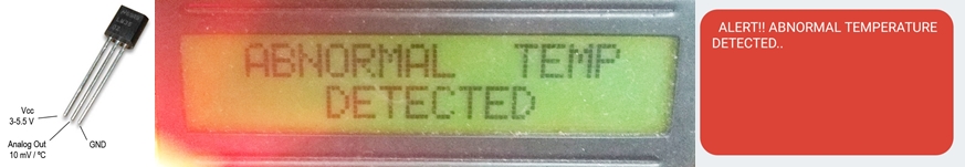
Fig. 3.2 Temperature module results
3.3 LUNGS ANALYZER MODULE
Yep—APA, Chicago, Harvard, MLA, Turabian, you name it! Our writers customize every detail to fit your assignment’s needs, ensuring it meets academic standards down to the last footnote or bibliography entry. They’re pros at making your paper look sharp and compliant, no matter the style guide.
These analysis is based on the inhaling power of the person. The infrared rays act as medium between the rise of the level and the inhaling capacity which holds the balls in the tube to indicate the level
Fig. 3.3 Lungs Health Analyser result
The healthy level and unhealthy conditions are sent in the form of message to the doctor immediately after the output displayed on LCD.
For sure—you’re not locked in! Chat with your writer anytime through our handy system to update instructions, tweak the focus, or toss in new specifics, and they’ll adjust on the fly, even if they’re mid-draft. It’s all about keeping your paper exactly how you want it, hassle-free.
4. COMPONENTS DESCRIPTION
4.1 POWER SUPPLY
A device or gadget that substances electrical or different varieties of power to an output load or group of hundreds is called an electricitysupply unit or PSU. The time period is maximum generally implemented to electrical strength resources, much less frequently to mechanical ones, and infrequently to others.
It’s a breeze—submit your order online with a few clicks, then track progress with drafts as your writer brings it to life. Once it’s ready, download it from your account, review it, and release payment only when you’re totally satisfied—easy, affordable help whenever you need it. Plus, you can reach out to support 24/7 if you’ve got questions along the way!
The term “strength deliver” is once in a while limited to those devices that convert a few other form of strength into electricity (together with sun strength and fuel cells and generators). An extra correct term for gadgets that convert one form of electric electricity into some other shape (together with transformers and linear regulators) is energy converter. The most common conversion is from AC to DC.
AQ regulated energy supply or stabilized energy supply is one that includes circuitry t Ao tightly manage the output voltage and/or modern to a specific price. The unique price is closely maintained no matter versions within the load presented to the strength deliver’s output, or any reasonable voltage variation on the energy supply’s input.
Fig. 4.1.1 Block diagram of power supply
Need it fast? We can whip up a top-quality paper in 24 hours—fully researched and polished, no corners cut. Just pick your deadline when you order, and we’ll hustle to make it happen, even for those nail-biting, last-minute turnarounds you didn’t see coming.
Rectifier:
The output from the transformer is fed to the rectifier. It converts A.C. into pulsating D.C. The rectifier may be a half wave or a complete wave rectifier. In this assignment, a bridge rectifier is used because it deserves to be a desirable balance amplifier in a circuit, which converts an ac voltage to dc voltage use of each half of cycles of the enter ac voltage. The Bridge rectifier circuit has four diodes linked to shape a bridge. The ac enter voltage is applied to the diagonally opposite ends of the bridge. The burden resistance is connected among the other ends of the bridge.
Fig. 4.1.2 Bridge Rectifier
For the wonderful 1/2 cycle of the enter ac voltage, diodes D1 and D3 conduct, while diodes. D2 and D4 continue to be in the OFF country. The conducting diodes will be in collection with the burden resistance RL and hence the weight present day flows via RL. For the bad half of cycle of the enter ac voltage, diodes D2 and D4 behaviour while, D1 and D3 stay OFF. The undertaking diodes D2 and D4 could be in collection with the burden resistance RL and therefore the present day flows via RL within the equal path as inside the preceding half cycle. Consequently a bi-directional wave is converted right into a unidirectional wave.
Absolutely—bring it on! Our writers, many with advanced degrees like Master’s or PhDs, thrive on challenges and dive deep into any subject, from obscure history to cutting-edge science. They’ll craft a standout paper with thorough research and clear writing, tailored to wow your professor.
Capacitive filter:
Capacitive filter out is used in this challenge. It removes the ripples from the output of rectifier and smoothens the D.C. Output received from this filter out is regular until the mains voltage and load is maintained regular. However, if either of the 2 is numerous, D.C. voltage acquired at this factor modifications. Consequently a regulator is carried out on the output stage.
Fig. 4.1.3 Rectified Output waveforms
Capacitive filter is used in this mission. It removes the ripples from the output of rectifier and will smoothens the D.C. Output obtained from this clear out is regular until the mains voltage and cargo is maintained consistent. However, if either of the 2 is various, D.C. voltage obtained at this point adjustments. Consequently a regulator is implemented on the output level.
We follow your rubric to a T—structure, evidence, tone. Editors refine it, ensuring it’s polished and ready to impress your prof.
Regulator:
The micro controller and other devices get strength supply from AC to DC adapter via voltage regulator. The adapter output voltage will be 12V DC non-regulated. The 7805/7812 voltage regulators are used to transform 12V to 5VDC.
As the call itself implies, it regulates the entered power to carry out. A voltage regulator is an electrical regulator designed to mechanically maintain a consistent voltage level. On this task, electricity supply of 5V and 12V are required. So as to obtain these voltage ranges, 7805 and 7812 voltage regulators are to be used. The primary range 78 represents high quality supply and the numbers 05, 12 constitute the specified output voltage tiers.
Send us your draft and goals—our editors enhance clarity, fix errors, and keep your style. You’ll get a pro-level paper fast.
4.2 ARM LPC2148 MICROCONTROLLER
The LPC2148 is a 64 pin microcontroller out of which forty six/forty eight pins are based on a 16-bit/32-bit ARM7TDMI-CPU with real-time emulation and embedded trace aid, that integrate microcontroller with embedded excessive pace flash memory ranging from 32 kB to 512 kB. A 128-bit wide memory interface and particular accelerator architecture allow 32-bit code execution on the maximum clock price. For essential code length programs, the opportunity 16-bit Thumb mode reduces code with the aid of more than 30 % with minimal performance penalty. Because of their tiny length and low power consumption, they are best for the applications where miniaturization is a key requirement, consisting of get right of entry to manage and point-of-sale.
Serial communications interfaces ranging from a USB 2.zero complete-pace tool, multiple UARTs, SPI, SSP to I2C-bus and on-chip SRAM of eight kB up to forty kB, make these devices thoroughly suitable for verbal exchange gateways and protocol converters, smooth modems, voice reputation and coffee give up imaging, presenting each big buffer length and high processing power. various 32-bit timers, individual or twin 10-bit ADC(s), 10-bit DAC, PWM channels and forty five speedy GPIO strains with as much as 9 side or level touchy outside interrupt pins make these microcontrollers appropriate for business manipulate and scientific systems.
Key features
4.2.1 Pin diagram and Description
Yep! We’ll suggest ideas tailored to your field—engaging and manageable. Pick one, and we’ll build it into a killer paper.
Fig. 4.2.1 Pin diagram of LPC2148
Port pin description
Table. 4.2.1.Port0 pin description
Table. 4.2.2 Port0 pin description
Yes! Need a quick fix? Our editors can polish your paper in hours—perfect for tight deadlines and top grades.
Table. 4.2.3 Port0 Pin Description
Table. 4.2.4 Port1 Pin Description
Table. 4.2.5 Port1 Pin description
Sure! We’ll sketch an outline for your approval first, ensuring the paper’s direction is spot-on before we write.
4.2.2 Functional Description
On-chip flash program reminiscence:
The LPC2148 includes a 32kB,64kB, 128kB,256kB and 512kB flash reminiscence device respectively. This reminiscence can be used for both code and facts garage. Programming of the flash memory may be executed in several approaches. It can be programmed in machine through serial port. The application software may erase and/or program the flash at the same time as the application is going for walks, permitting a top notch degree of flexibility for information storage subject firmware improvements, etc., Due to architectural solution selected for an on-chip boot loader, flash reminiscene to be had for consumers code on LPC2148 flash memory affords at least 100,000 erase/write cycles and twenty years of statistics retention.
On-chip static RAM:
On-chip static RAM may be used for code and/or information garage. The SRAM may be accessed as 8-bit, sixteen-bit, and 32-bit. LPC2148 provide eight kB, sixteen kB and 32 kB of static RAM respectively. In case of LPC2146/48 simplest, an 8 kB SRAM block meant to be applied especially by way of the USB can also be used as a fashionable reason RAM for facts storage and code storage and execution.
Interrupt Controller:
The Vectored Interrupt Controller (VIC) accepts all the interrupt request inputs and categorizes them as fast Interrupt Request (FIQ), vectored Interrupt Request (IRQ), and non-vectored IRQ as defined by means of programmable settings. The programmable mission scheme method that priorities of interrupts from the numerous peripherals can be dynamically assigned and adjusted. rapid interrupt request (FIQ) has the best priority. If a couple of request is assigned to FIQ, the VIC combines the requests to provide the FIQ sign to the ARM processor. The fastest possible FIQ latency is completed when most effective one request is classified as FIQ, due to the fact then the FIQ service ordinary does now not want to branch into the interrupt carrier ordinary however can run from the interrupt vector area.
Definitely! Our writers can include data analysis or visuals—charts, graphs—making your paper sharp and evidence-rich.
If more than one request is assigned to the FIQ magnificence, the FIQ service ordinary will examine a phrase from the VIC that identifies which FIQ source(s) is (are) asking for an interrupt. Vectored IRQs have the middle precedence. sixteen of the interrupt requests can be assigned to this category. Any of the interrupt requests may be assigned to any of the 16 vectored IRQ slots, among which slot zero has the best precedence and slot 15 has the bottom. Non-vectored IRQs have the bottom priority. The VIC combines the requests from all the vectored and non-vectored IRQs to supply the IRQ sign to the ARM processor.
The IRQ carrier ordinary can start with the aid of reading a check in from the VIC and leaping there. If any of the vectored IRQs are pending, the VIC gives the address of the very best-precedence asking for IRQs service ordinary, in any other case it gives the deal with of a default routine that is shared by means of all the non-vectored IRQs. The default recurring can read every other VIC sign in to peer what IRQs are energetic.
Interrupt assets:
Each peripheral tool has one interrupt line linked to the Vectored Interrupt Controller, but might also have numerous inner interrupt flags. Personal interrupt flags might also represent a couple of interrupt supports.
Pin connect block:
The pin connect block lets in selected pins of the microcontroller to have multiple characteristic. Configuration registers manage the multiplexers to permit connection between the pin and the on chip peripherals. Peripherals ought to be related to the perfect pins previous to being activated, and previous to any related interrupt(s) being enabled. Pastime of any enabled peripheral characteristic that isn’t mapped to a associated pin have to be considered undefined. The Pin manipulate Module with its pin select registers defines the functionality of the microcontroller in a given hardware environment. After reset all pins of Port 0 and 1 are configured as input with the subsequent exceptions: If debug is enabled, the JTAG pins will count on their JTAG capability; if hint is enabled, the hint pins will assume their trace capability. The pins related to the I2C0 and I2C1 interface are open drain.
Speedy general cause parallel I/O (GPIO):
Tool pins that aren’t connected to a particular peripheral function are controlled with the aid of the GPIO registers. Pins may be dynamically configured as inputs or outputs. Separate registers permit placing or clearing any number of outputs concurrently. The cost of the output sign up may be read again, as well as the modern-day kingdom of the port pins. LPC2148 introduce multiplied GPIO functions over previous LPC2000 gadgets:
10 Bit ADC:
The LPC21418 comprise one analog to virtual converters. Those converters are 10-bit successive approximation analog to virtual converters. At the same time as ADC0 has six channels, ADC1 has eight channels. Consequently, general variety of available ADC inputs for LPC2148 is 14. The LPC2148 contain two analog to virtual converters. Those converters are single 10-bit successive approximation analog to digital converters. While ADC0 has six channels, ADC1 has eight channels. Consequently, overall variety of to be had ADC inputs for LPC21418 is 14.
We’ve got it—each section delivered on time, cohesive and high-quality. We’ll manage the whole journey for you.
Capabilities:
10 bit DAC
The DAC enables the LPC2148 generate a variable analog output. The maximum DAC output voltage is the VREF voltage.
Yes! UK, US, or Aussie standards—we’ll tailor your paper to fit your school’s norms perfectly.
Functions:
USB 2.zero tool controller:
The USB is a 4-cord serial bus that supports communique between a host and a number of (127 max) of peripherals. The host controller allocates the USB bandwidth to attached devices via a token based totally protocol. The bus supports warm plugging, unplugging, and dynamic configuration of the gadgets. All transactions are initiated by the host controller. The LPC2148 is prepared with a USB tool controller that enables 12 Mbit/s information exchange with a USB host controller. It consists of a sign up interface, serial interface engine, endpoint buffer memory and DMA controller.
The serial interface engine decodes the USB data stream and writes statistics to the best give up factor buffer reminiscence. The status of a finished USB switch or blunders situation is indicated thru status registers. An interrupt is likewise generated if enabled. A DMA controller (to be had in LPC2146/48 only) can switch facts between an endpoint buffer and the USB RAM.
UART:
If your assignment needs a writer with some niche know-how, we call it complex. For these, we tap into our pool of narrow-field specialists, who charge a bit more than our standard writers. That means we might add up to 20% to your original order price. Subjects like finance, architecture, engineering, IT, chemistry, physics, and a few others fall into this bucket—you’ll see a little note about it under the discipline field when you’re filling out the form. If you pick “Other” as your discipline, our support team will take a look too. If they think it’s tricky, that same 20% bump might apply. We’ll keep you in the loop either way!
The LPC2148eight each comprise two UARTs. In addition to standard transmit and obtain statistics traces, the LPC2148 UART1 also gives a full modem control handshake interface. in comparison to previous LPC2000 microcontrollers, UARTs in LPC2148 introduce a fractional baud charge generator for each UARTs, allowing these microcontrollers to attain general baudrates such as 115200 with any crystal frequency above 2MHz. similarly, automobile-CTS/RTS flow-manipulate capabilities are absolutely carried out in hardware.
Features:
LPC2148 contains I2C-bus controllers. The I2C-bus is bidirectional, for inter-IC manage the usage of most effective two wires: a serial clock line (SCL), and a serial facts line (SDA). every tool is recognized by a unique deal with and can operate as either a receiver-only device (e.g., an lcd driver or a transmitter with the functionality to both receive and ship facts (inclusive of memory)). Transmitters and/or receiver scan perform in both master or slave mode, depending on whether or not the chip has to initiate a records switch or is best addressed. The I2C-bus is a multi-master bus, it could be controlled by means of a couple of bus grasp connected to it. The I2C-bus carried out in LPC2141/forty two/44/forty six/48 helps bit fees up to 400 kbit/s (speedy I2C-bus).
Functions:
Our writers come from all corners of the globe, and we’re picky about who we bring on board. They’ve passed tough tests in English and their subject areas, and we’ve checked their IDs to confirm they’ve got a master’s or PhD. Plus, we run training sessions on formatting and academic writing to keep their skills sharp. You’ll get to chat with your writer through a handy messenger on your personal order page. We’ll shoot you an email when new messages pop up, but it’s a good idea to swing by your page now and then so you don’t miss anything important from them.
SPI serial I/O controller:
The LPC2148 comprise one SPI controller. The SPI is a full duplex serial interface, designed to address more than one masters and slaves related to a given bus. Simplest a single master and a single slave can communicate on the interface in the course of a given records switch. Throughout an information switch the grasp always sends a byte of statistics to the slave, and the slave continually sends a byte of records to the grasp.
Features
Crystal oscillator
On-chip integrated oscillator operates with outside crystal in range of one MHz to twenty-five MHz. The oscillator output frequency is called fosc and the ARM processor clock frequency is referred to as CCLK for functions of charge equations, and so on. fosc and CCLK are the equal cost except the PLL is going for walks and related. check with phase 6.19.2 “PLL” for extra records.
PLL
The PLL accepts an enter clock frequency in the range of 10 MHz to twenty-five MHz. The input frequency is extended up into the variety of 10 MHz to 60 MHz with a modern managed Oscillator (CCO). The multiplier may be an integer fee from 1 to 32 (in exercise, the multiplier cost can’t be higher than 6 on this family of microcontrollers due to the upper frequency restriction of the CPU). The CCO operates within the range of 156 MHz to 320 MHz, so there is an additional divider within the loop to keep the CCO within its frequency range even as the PLL is presenting the preferred output frequency. The output divider may be set to divide with the aid of 2, four, eight, or sixteen to produce the output clock. for the reason that minimal output divider value is two, it’s miles insured that the PLL output has a 50 % obligation cycle. The PLL is turned off and bypassed following a chip reset and may be enabled through software. this system must configure and set off the PLL, anticipate the PLL to fasten, then connect with the PLL as a clock supply. The PLL settling time is 100 µs.
Reset and wakeup timer:
Reset has sources at the LPC2141/forty two/forty four/46/forty eight: the RESET pin and watchdog reset. The RESET pin is a Schmitt trigger enter pin with a further glitch filter out. assertion of chip reset through any source begins the Wake-up Timer (see Wake-up Timer description underneath), causing the inner chip reset to remain asserted till the external reset is de-asserted, the oscillator is walking, a set quantity of clocks have surpassed, and the on-chip flash controller has finished its initialization. While the inner reset is eliminated, the processor starts executing at cope with 0 that is the reset vector. At that point, all of the processor and peripheral registers have been initialized to predetermined values. The Wake-up Timer guarantees that the oscillator and other analog features required for chip operation are absolutely practical before the processor is allowed to execute instructions. This is important at energy on, all varieties of reset, and every time any of the aforementioned features are turned off for any cause. for the reason that oscillator and other capabilities are turned off throughout energy-down mode, any wake-up of the processor from strength-down mode uses the Wake-up Timer. The Wake-up Timer video display units the crystal oscillator because the means of checking whether or not it’s far secure to begin code execution. When strength is applied to the chip, or a few occasion caused the chip to exit power-down mode, while is needed for the oscillator to supply a sign of enough amplitude to force the clock logic. the amount of time relies upon on many elements, such as the price of VDD ramp (in the case of strength on), the kind of crystal and its electrical characteristics (if a quartz crystal is used), as well as any other outside circuitry (e.g. capacitors), and the characteristics of the oscillator itself beneath the prevailing ambient conditions.
External interrupt inputs:
LPC2148 includes up to 9 facet or stage sensitive external Interrupt Inputs as selectable pin capabilities. When the pins are combined, outside occasions may be processed as 4 independent interrupt signals. The outside Interrupt Inputs can optionally be used to wake-up the processor from electricity-down mode. Moreover capture input pins also can be used as outside interrupts without the option to wake the tool up from strength-down mode.
RS232 CABLE:
To permit compatibility amongst statistics communication gadget, an interfacing preferred known as RS232 is used. considering the standard was set long before the appearance of the TTL logic family, its enter and output voltage tiers are not TTL compatible. for that reason, to attach any RS232 to a microcontroller system, voltage converters together with MAX232 are used to convert the TTL logic degrees to the RS232 voltage stages and vice versa.
4.3 EEPROM
EEPROM is a memory storing device which is used widely because of its features. The data can be erased electrically as the name notates electrically erasable memory device. The memory storage capacity of this tiny device is 4kb and it is re used based on the requirement
Fig. 4.3 EEPROM
The data stored by this EEPROM is the registered number and the receiving mobile number which includes the information of the medicines prescribed by the doctor and the message sent to the doctor in the detection of abnormal conditions.
4.4 MAX232
Max232 IC is a specialized circuit which makes standard voltages as required with the aid of RS232 standards. This IC affords first-class noise rejection and really reliable against discharges and brief circuits. MAX232 IC chips are typically referred to as line drivers.
Fig. 4.4 MAX232 IC
 To make sure facts switch between pc and microcontroller, the baud rate and voltage degrees of Microcontroller and computer have to be the equal. The voltage degrees of microcontroller are logic1 and common sense 0 i.e., common sense 1 is +5V and good judgment zero is 0V. But for laptop, RS232 voltage ranges are considered and they’re: good judgment 1 is taken as -3V to -25V and logic 0 as +3V to +25V. So, so one can identical these voltage degrees, MAX232 IC is used. As a consequence this IC converts RS232 voltage stagesto microcontroller voltage levels and vice versa.
4.5 SWITCHES
A switch array is used to select the age of the person. Depending on the age of the person the value is given and if the output value is different. Initially the switch is selected so that the microcontroller reads the value and displays the output in normal and abnormal conditions.
Fig. 4.5 Switch array
4.6 LCD
LCD is the combination of two states which is solid and liquid state and is used to display a visible image of characters.
Fig. 4.6 LCD display
This indicates that the LCD is ready to display the output if the health condition and the message sent from the doctor is also displaye don LCD. This type of LCD displays 16×2 characters.
5. ECG MODULE
5.1 ECG WORKING
A record which displays a graphical waveformsof a person heart beat is represented in the form of ECG. Heart is unique magic muscle which is an intrinsic conduction system where the ability if creating impulses is carried out by its own without any type of influence from outside.
When these electrical impulses are occurring in heart it creates a current which is spread to the body and they reach skin. The complete number of impulses are calculated and graphed in the form of ECG.
An ECG test is performed by placing electrodes on the skin where they are interacted with the electrical impulses in the body. AS these electrical impulses pass from artria to ventricles then there is variation between electrodes and the performance of heart function is obtained.
In an ECG there are three distinct waves which indicate the heart functioning. These three waves named as P wave, QRS wave, T wave together represent the functioning of heart beat.
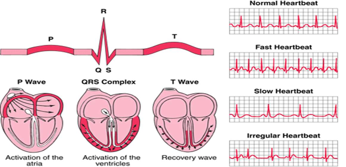
Fig. 5.1.1 ECG Representation
The variation in these waves describes the heart heath condition of the person. The different conditions of heart is observed from the distance between these waves and the condition if the person is analysed. With a view to be capable of report myocardial activity, the electrocardiograph desires if you want to stumble on tiny modifications in capacity at the frame surface. We are talking about signals which can be frequently around 1mV, and may be smaller. Similarly, we need a few reference point to which we relate the capability modifications.
This is measured by connecting the electrodes to the body. The 12-lead ECG is used to find the heartbeat, over time there are several systems developed that make up to 12-lead ECG. They are:

Fig. 5.1.2 Bipolar leads placement

Fig. 5.1.3 Unipolar leads placement 1
Fig. 5.1.4 Unipolar leads placement 2

Fig. 5.1.5 V leads placement
We can visualise the directions of the various leads — I factors left, and aVF points immediately down (in a ‘Southward’ route). The alternative leads are organized around the points of the compass — AVL approximately 30o more north of I, II down toward the left foot, about 60o south of I, and III off to the right of AVF. AVR `looks’ on the coronary heart from up and right, so efficiently it is seeing the chambers of the heart, and maximum deflections in that lead are poor (internet high-quality vector in AVR is uncommon, and suggests that lead placement was incorrect. If the leads had been successfully sited, then assume dextrocardia or some different unusual congenital abnormality).
Fig. 5.1.6 Visulization of LED’s
It is normal to organization the leads in step with which part of the left ventricle (LV) they examine. AVL and that i, in addition to V5 and V6 are lateral, while II, III and AVF are inferior. V1 thru V4 have a tendency to observe the anterior factor of the LV (a few check with V1 and V2 `septal’, however a higher call is perhaps the `proper oriented leads’). changes in depolarisation within the posterior aspect of the coronary heart aren’t directly visible in any of the conventional leads, even though “replicate photo” adjustments will tend to be picked up in V1 and V2.
ECG paper is traditionally divided into 1mm squares. Vertically, ten blocks generally correspond to at least one mV, and on the horizontal axis, the paper pace is usually 25mm/s, so one block is 0.04s (or 40ms). notice that we also have “huge blocks” which might be 5mm on their aspect.
Fig. 5.1.7 Paper presentation
Always check the calibration voltage on the right of the ECG, and paper velocity. the following picture suggests the everyday 1mV calibration spike.
Fig.5.1.8 ECG graphical presentation
5.2 ECG CONDITIONS
1. Sinus bradycardia
Aside from healthy, however in any other case everyday people, there may be a protracted list of conditions where sinus bradycardia happens, along with:
2. Sinus Tachycardia
Continually remember pain as a likely purpose of tachycardia.
If the rate is almost exactly 150, always make sure that you are not mistaking atrial flutter with a 2:1 block for sinus tachycardia.
Rhythm
 Sinus arrhythmia and heart price variability
There’s commonly a mild diploma of chaotic variant in heart rate, known as sinus arrhythmia. Sinus arrhythmia is usually a good element, and lack of this chaotic variant is of ominous prognostic significance. Submit myocardial infarction, a metronome-like regularity of the pulse is associated with an accelerated likelihood of unexpected demise, and simply before the onset of ventricular tachycardia (or fibrillation), variability is lost! Absence of any sinus arrhythmia indicates an autonomic neuropathy.
Fig. 5.2.1 Sinus arrhythmia representation
These rise up from ectopic atrial foci. Commonly, the ectopic beat always arises at about the identical time after the sinus beat.
Fig .5.2.2 Atrial extra systoles representation
The ectopic beat commonly discharges the SA node, so subsequent beats of SA foundation aren’t in synchrony with the previous sinus rhythm.
If the extrasystole takes place early on, it may discover the His-Purkinje gadget no longer quite prepared to get hold of an impulse, and a diploma of block can be visible. That is termed `aberration’. Distinguish between an atrial extrasystole, and an atrial break out beat, wherein the SA node falters, and a subsidiary pacemaker takes over.
Supraventricular tachyarrhythmias (SVT)
Irregular SVT
 By way of far the most typical purpose of irregular SVT is atrial traumatic inflammation, in which the atrial price is inside the location of 450 to 600/min, and the atria honestly do now not contract rhythmically in any respect. The atrium “fibrillates”, writhing like a bag of worms. The conventional view of the pathogenesis of AF is that there are multiple re-entrant `wavelets’ shifting thru the atrial muscle, however recent proof suggests that plenty AF honestly arises from ectopic interest inside the muscular cuff surrounding the pulmonary veins where they enter the left atrium. AF is concept to beget further AF thru “electrical remodelling” — electrophysiological changes that are induced in atrial myocytes due to fast rates and the consequent calcium loading.
Fig.5.2.3 Irregular SVT
Note that in the above tracing of AF, the ventricular response rate seems rather slow, so we suspect that AV block has been increased using pharmacological manipulation. In uncontrolled AF, rates of about 130 or more are common.
Other causes of irregular SVT are:
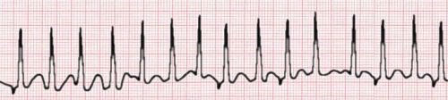
Fig . 5.2.4 Irregular SVT in other case
Although it looks like atrial fibrillation, the above image actually shows multifocal atrial tachycardia. Note how there are at least three different P wave configurations!
A trial flutter is common. The atrial rate is commonly 300/min, and there is usually a 2:1 block, resulting in a ventricular response rate of 150/min. Other ratios are possible, and sometimes the ratio varies. This rhythm is often unstable, and the heart may flip in and out of sinus rhythm, or there may be runs of atrial fibrillation.
Tags: Affordable Online College Homework, Cheap essay writer Australia, Pay someone to write my paper, Research Essay Help UKYou Want The Best Grades and That’s What We Deliver
Our top essay writers are handpicked for their degree qualification, talent and freelance know-how. Each one brings deep expertise in their chosen subjects and a solid track record in academic writing.
We offer the lowest possible pricing for each research paper while still providing the best writers;no compromise on quality. Our costs are fair and reasonable to college students compared to other custom writing services.
You’ll never get a paper from us with plagiarism or that robotic AI feel. We carefully research, write, cite and check every final draft before sending it your way.